
E-Plane Throttle Quadrant — Controller Board Revision Report
c457569
Current
458fdbf
Executive summary
This is a targeted reliability and manufacturability revision of the board previously prototyped at c457569. It separates the MCP25625 CAN controller from the shared SPI bus, cleans the copper routing standard, and tightens local power and clock placement—while preserving the board outline, connector plan, component count, and low-cost two-layer construction.
What changed — and why
Electrical comparisons come from the KiCad schematic and PCB at the two exact commits; dimensions and route counts were read directly from the board database.
Dedicated CAN-controller SPI
MCP25625 pins 14–16 moved from shared SCK/MOSI/MISO to CAN_SCK/CAN_MOSI/CAN_MISO, using ESP32-S3 GPIO 5, 21 and 41. The display and MA730 remain on the original bus.removes CAN traffic from the multi-device SPI path, reducing bus-contention risk and simplifying firmware timing and recovery.
Disciplined signal routing
New routing was normalized to 45° geometry and a short metric width palette. Legacy 0.254 / 0.381 / 0.508 / 0.635 mm widths were removed; CAN SPI is fixed at 0.15 mm, with 0.20 / 0.25 mm used for general signals and wider copper reserved for power.makes each route’s electrical intent obvious and prevents unexplained width changes inside ordinary signal runs.
Regulator decoupling placement
C5, the +12 V input bulk capacitor, moved 13.77 mm and flipped to the bottom side beside U1. C2, the +5 V output bulk capacitor, moved 8.77 mm to the regulator output area.shortens the input/output current loops around the R-78E regulator and improves transient and conducted-noise behavior.
CAN clock and local bypass cleanup
Y1 moved 0.50 mm toward U5; C9 moved 0.50 mm and C10 moved 1.00 mm toward their loads. Both MCP25625 oscillator routes were made consistently 0.25 mm.reduces critical loop area and keeps the 16 MHz clock and local supply return paths compact and predictable.
Fabrication rules with margin
Global minimum track width increased from 0.10 to 0.15 mm. Minimum via changed from 0.35 / 0.20 mm to 0.60 / 0.30 mm, while copper-to-edge remains 0.508 mm. A scoped 0.10 mm clearance applies only to the three dedicated CAN SPI nets.keeps the dense route on a standard 1 oz, two-layer process while using more robust drills and annular copper everywhere else.
Auditable design baseline
The repository now carries a formal review package: BOM, Gerbers, drill and placement files, PCB/schematic PDFs, STEP model, DRC/ERC reports, SKiDL source/netlists, and the design-review record.gives future revisions a reproducible manufacturing reference instead of relying on an editor state or a single production zip.
This spin does not change the footprint set, connector map, mounting pattern, board envelope, or layer count. It is a focused controller-interface and layout-quality revision—not a product-certification or full protection-architecture redesign.
Physical revision comparison
Render note: all connector bodies are displayed for mechanical clarity. J1, J2, J6 and J8 remain marked DNP in the current KiCad source; only the render-only copy was unhidden.
Top side
Drag center handle to compare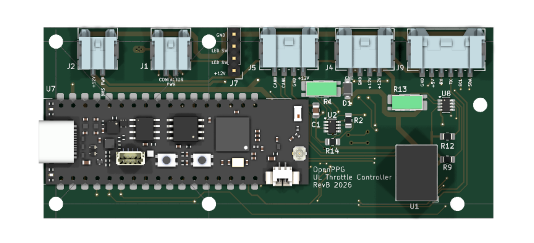
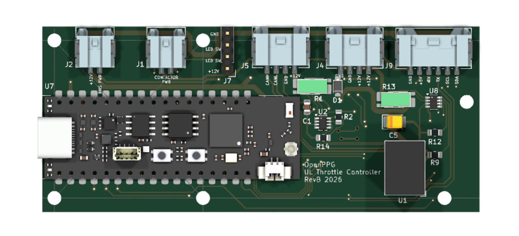 Before · c457569
After · 458fdbf
Before · c457569
After · 458fdbf
Bottom side
Drag center handle to compare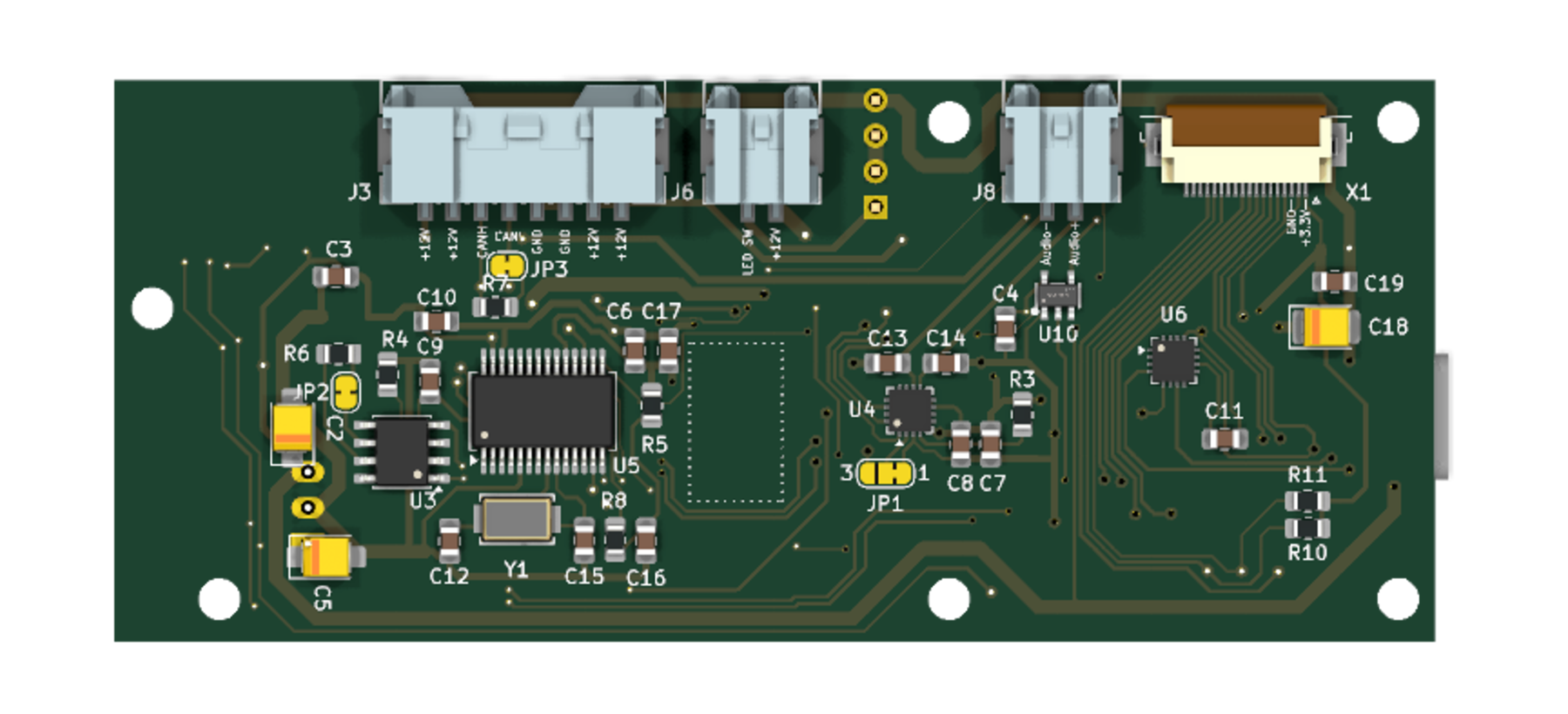
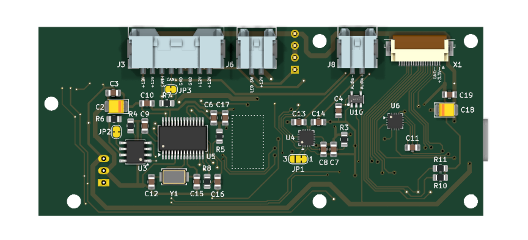 Before · c457569
After · 458fdbf
Before · c457569
After · 458fdbf
Validation & manufacturing readiness
Revision 2 engineering addendum · 2026-07-13 · post-458fdbf candidate
Protection, deterministic startup and CAN SPI integrity
The first revision separated and cleaned the CAN-controller interface. This follow-on closes the lowest-cost electrical risks discovered during review: the 12 V rail now has a real transient suppressor and correctly rated bulk capacitor, the MCP25625 has defined chip-select and firmware-controlled reset states, and the two ESP32-driven CAN SPI outputs have source damping. The design remains a 2-layer, 1 oz, 1.6 mm board; these are targeted component-and-routing changes rather than a cost-driving architecture change.
What was added—and the failure mode each change addresses
Every added part has a specific job. The goal is not to make the board immune to every possible vehicle or bench fault; it is to remove avoidable single-point weaknesses in the intended 12 V prototype envelope and make the remaining limits explicit.
Clamp the +12 V rail before the regulator sees the cable energy
The previous board relied on a 10 µF / 16 V bulk capacitor and the regulator’s own 28 V input envelope. Harness inductance can convert an ordinary hot-plug edge into a much higher rail peak, so a 16 V capacitor had no useful margin even on several 16 V test corners.
Implemented: D2 is an SMAJ15A TVS in an SMA / DO-214AC package from +12V to GNDD; C5 remains 10 µF but is upgraded to 35 V. The local TVS, C5 and regulator feed use 1.0 mm, 45°/orthogonal copper. The PCB footprint value was also synchronized to 10uF 35V so board and schematic BOM data agree.
Keep the MCP25625 inactive until firmware deliberately enables it
A floating chip-select can be interpreted as an SPI transaction while the ESP32 pins are still high-impedance. The original passive reset network also cannot guarantee a fresh reset after every slow or disturbed power ramp.
Implemented: R15 is 10 kΩ from LDO2_3V3 to MCP_CS. MCP reset is now connected to ESP32-S3 GPIO42 while retaining R5 = 10 kΩ, C16 = 100 nF and R8 = 2 kΩ. Firmware can now force reset low after boot and after detected power faults.
Damp the two fast source-driven CAN SPI edges
The dedicated bus is electrically cleaner than the shared bus, but the routed SCK path is still 64.554 mm with seven vias. With fast ESP32 edges, that path can ring even when protocol timing is correct. MOSI is shorter, but still long enough to benefit from modest source damping.
Implemented: R16 = 33 Ω splits CAN_SCK from CAN_SCK_U5; R17 = 22 Ω splits CAN_MOSI from CAN_MOSI_U5. Both are located at the ESP32 source under the socketed ProS3 module. MISO remains undamped because its source is the MCP25625 at the opposite end.
Correct the auxiliary connector net and preserve the cheap stack-up
J6 pad 2 was aligned with schematic J7 pin 1 so the PCB no longer carries a connector-net mismatch. CAN SPI remains 0.15 mm with a tightly scoped 0.10 mm clearance rule; the two new resistors receive only the courtyard exception needed beneath U7.
Why this matters: the fix prevents a documentation-to-copper surprise at assembly, while the scoped rules avoid relaxing the rest of the board. The retained 0.60 / 0.30 mm minimum via, 0.508 mm copper-to-edge clearance and 1 oz 2-layer construction remain comfortably inside JLCPCB’s published 2-layer capabilities.
Before / after simulation evidence
These comparisons are not generic calculations: they use the revised component values and actual routed CAN SPI lengths and via counts. The labels show the exact measured outputs used for the order decision.
Worst regulator-input hot-plug peak by source voltage
highest of 9 harness R/L corners per source · voltsCAN SPI raw-envelope flags
flagged corners out of 17 · fewer is betterMCP startup control
3.3 V logic thresholdsMCP_CS during ESP32 high-impedance boot
RESET asserted after a disturbed rail
MISO physical setup margin
minimum modeled margin · nanosecondsProtection stress tests
magnitude at protected +12 V railThe new reproducible SPICE validation setup
The useful output of this revision is not only the four added parts. The repository now contains a repeatable pre-order simulation harness under simulation/. A single aggregate runner executes power/protection, MCP25625 sequencing/reset and routed CAN SPI studies, retains the reviewed findings, and exits nonzero whenever an operating, firmware or bench-validation gate remains open.
Harness energy, regulator margin and fault polarity
Four core ngspice decks cover hot-plug/load steps, brownout, inlet reverse polarity plus a +35 V screening pulse, and reverse drive applied after the inlet diode. A generated matrix then sweeps 8, 12, 16, 24 and 28 V sources against 20 / 100 / 500 mΩ harness resistance and 0.2 / 2 / 10 µH harness inductance.
Design feedback: the baseline peaks justified D2 and the 35 V C5 upgrade. Re-running the same matrix quantified exactly where the revised clamp succeeds and where the regulator remains outside specification.
Rail order, boot-state and unpowered-I/O behavior
Nine decks exercise the actual ProS3 GPIO17-controlled LDO2 startup, +5 V first, 3.3 V first, a 20 ms slow ramp, nonmonotonic recovery below the 2.4 V retention threshold, a 100 µs brownout, ESP32 high-impedance CS boot, GPIO42 reset assertion/release, and an SPI input driven while U5 is unpowered.
Design feedback: this suite directly produced R15 and the GPIO42 reset connection. The official ProS3 schematic then replaced the generic normal-startup source with its real U2 NCP167 regulator, VDD_SPI AND GPIO17 enable path and 1 µF output capacitor. It also proved that the passive RC cannot be the only recovery mechanism and converted that discovery into explicit firmware requirements.
Actual trace geometry, edge damping and timing margin
The transmission-line decks use the routed SCK/MOSI/MISO lengths and via counts, then sweep source impedance, 0 / 22 / 33 / 47 Ω series resistance, 80–180 Ω line impedance, 1–5 ns edge rate and 5–15 pF receiver loading. The ProS3 schematic confirms that GPIO5/SCK and GPIO21/MOSI reach the headers directly with no hidden series resistors or translators. Node-based post-processing scores ringing and MISO setup margin.
Design feedback: the results selected 33 Ω for SCK, 22 Ω for MOSI and an 8 MHz initial firmware clock. The same suite can be rerun if resistor values or routing change.
Reproducibility: run ./simulation/run_all.sh with ngspice 46 or newer and Node.js. Generated decks, logs and waveforms are regenerated locally; the reviewed assumptions and result summaries stay with the design. The models are deliberately conservative and are release screens—not substitutes for probing the assembled board.
Findings addressed in this PCB revision
- 16 V C5 lacked hot-plug marginC5
Several baseline 16 V corners exceeded the capacitor rating; C5 is now 10 µF / 35 V in both schematic and PCB metadata.
- No dedicated +12 V transient clampD2
Harness inductance produced peaks as high as 41.57 V from a 24 V source and 48.62 V from 28 V. D2 now shunts the event locally.
- MCP_CS was undefined during ESP32 bootR15
R15 establishes a guaranteed inactive state instead of depending on pin startup behavior.
- Reset recovery was not firmware-controllableGPIO42
GPIO42 can now assert and release MCP_RESET against the retained RC network.
- SCK and MOSI showed excessive raw ringing flagsR16/R17
Source termination reduces flagged SCK corners from 11 to 7 and MOSI corners from 9 to 6.
Findings still open—or conditional on product requirements
- 28 V and low-impedance +35 V sources remain outside U1’s envelopeFuture HW
Two 28 V hot-plug corners reach above 28 V and the +35 V pulse clamps at 31.455 V. If that becomes a real requirement, use a higher-voltage regulator or a proper surge/eFuse front end in a later spin.
- 8 V does not sustain a valid +5 V railSpec choice
All nine 8 V corners fail the 4.75 V output gate after harness, shunt and diode drops. Only redesign the power stage if 8 V operation is required.
- The passive reset RC misses disturbed-rail reset guaranteesFirmware
Firmware must pulse GPIO42 after initialization and detected supply faults. A voltage supervisor is the hardware option if software recovery is not sufficient.
- Driving SPI into an unpowered MCP25625 exceeds the I/O limitFirmware
SCK, MOSI and CS must stay low or high-impedance while U5 is off. Add isolation only if power sequencing cannot be guaranteed in firmware.
- LDO2 is explicitly software-gated by ProS3 GPIO17Firmware
Configure GPIO17 as an output, enable LDO2, wait conservatively before pulsing GPIO42, then configure CAN SPI. Use 1 ms initially and verify on hardware; 120 µs is a typical value, not a guaranteed maximum.
- Conservative SPI ringing flags remain after dampingBench
The resistor values are supported by the model, but final values require scope measurements at both ends of each line. Adjust stuffing if the real edge is materially different.
- 10 MHz has only 1.47 ns of modeled physical MISO marginFirmware
Start at 8 MHz, where the modeled margin is 13.97 ns. Treat 10 MHz as an optional bench-qualified optimization, not the default.
Exact validation results and release interpretation
The aggregate suite intentionally returns a nonzero release gate when a test defines a remaining operating or firmware restriction. A “limit” below is therefore useful design information, not a simulator crash.
| Category | Exact result | Interpretation | Status |
|---|---|---|---|
| Nominal 12 V power | +5 V = 4.9197–4.9960 V through 50 mA, 800 mA and 1.02 A tested loads | Hot-plug and load-step regulation remains inside the 4.75–5.25 V gate. | Pass |
| 12 / 16 / 24 V hot-plug | Worst peaks = 18.9456 / 21.2203 / 26.9588 V; 0 of 27 corners over 28 V | The TVS materially protects the regulator in the intended and adjacent source ranges. | Pass |
| 28 V hot-plug | Worst peak = 30.1443 V; 2 of 9 corners over U1’s 28 V envelope | Do not advertise or test this design as a 28 V-qualified input. | Limit |
| 8 V input | All 9 corners fail the 4.75 V output gate | Harness, shunt and diode drops leave insufficient headroom for the R-78E model. | Limit |
| Positive screening pulse | +35 V source produces 31.4554 V at C5/U1; C5 passes 35 V rating, U1 exceeds 28 V | The TVS protects the capacitor but cannot guarantee regulator survival for an arbitrary low-impedance 35 V source. | Limit |
| Reverse input | J5-protected reverse = −0.0281 V; direct post-diode reverse = −0.8545 V with 1 Ω source | D1 protects the intended inlet; D2 also limits accidental reverse drive on connectors tied directly to +12 V. | Pass |
| Brownout recovery | 12 → 8 → 6 → 12 V sequence recovers +5 V to 4.9682 V | The power rail recovers, but firmware must still reinitialize the MCP25625. | Pass |
| ProS3 LDO2 startup | Off before GPIO17; modeled 95% point = 120.902 µs; final rail = 3.2998 V; CS = 3.2897 V after settling | The official U2/AND-gate topology satisfies the typical-startup model. Firmware still uses a conservative delay because the data sheet gives no maximum turn-on time. | Pass |
| MCP_CS boot state | R15 holds 3.28999 V minimum versus 2.31 V guaranteed-high threshold | U5 remains deselected while the ESP32 pin is high-impedance. | Pass |
| GPIO42 reset | Asserted = 0.00905 V; released = 3.300 V; thresholds are ≤0.495 V and ≥2.805 V | Firmware has ample electrical margin to force and release reset. | Pass |
| Passive reset recovery | Slow-ramp low-margin = +2.1303 V; nonmonotonic recovery = 2.2592 V; brownout recovery = 1.8562 V | The RC alone does not guarantee a new reset after all disturbed-rail cases. | Firmware |
| Unpowered U5 SPI pin | Modeled over-VDD stress = 0.6002 V versus 0.300 V absolute-maximum allowance | Keep SCK, MOSI and CS low or high-impedance whenever MCP25625 power is absent. | Firmware |
| CAN SPI sweep | 204 total corners; 51 as-built; SCK 7 flags, MOSI 6, MISO 6 | Series resistors improve the two driven outputs, but assembled-board scope correlation remains required. | Bench check |
What the simulations can—and cannot—prove
- RECOM does not publish an R-78E transistor-level SPICE macro-model. The power converter is a documented rail-level behavioral envelope and does not predict internal switching ripple, loop stability or survival beyond 28 V.
- The SMAJ15A model follows its standoff, breakdown and clamping envelope. Real clamp voltage depends on the selected manufacturer, pulse shape, layout inductance and source impedance.
- The ProS3 lacks a board-level IBIS model. SPI uses conservative source impedance, line impedance, edge-rate and load-capacitance corners; unclamped peaks identify stress and EMI sensitivity.
- The official ProS3 Rev P4 schematic does expose the power topology: U2 is an NCP167BMX330TBG enabled by VDD_SPI AND GPIO17, with 1 µF input/output capacitance. The exact B variant has no active output discharge, so shutdown decay remains load-dependent.
- The NCP167 startup deck uses its data-sheet typical 120 µs-to-95% value. It validates the expected normal sequence but is not a transistor-level control-loop, dropout or load-transient model.
- The MCP25625 sequencing decks use datasheet thresholds and representative input clamps, not an unpublished internal POR macro-model.
Prototype order gate
Proceed for a nominal 12 V prototype with the revised C5/D2 protection, R15 pull-up, GPIO42 reset path and 33 Ω / 22 Ω source resistors populated.
- Firmware starts CAN SPI at 8 MHz.
- Firmware configures GPIO17 as an output, enables ProS3 LDO2, waits 1 ms initially for the 3.3 V rail to settle, then pulses GPIO42 low before starting CAN SPI.
- Firmware pulses GPIO42 low after initialization and after power-fault recovery.
- Firmware does not drive MCP SPI pins while U5 is unpowered.
- Bench validation captures +12 V, +5 V, SCK, MOSI and MISO using short ground springs during hot-plug, maximum load and CAN traffic.
- 28 V and arbitrary +35 V source operation remain outside the qualified envelope.
Engineering sources: Unexpected Maker ProS3 Rev P4 schematic · onsemi NCP167 datasheet · Espressif ESP32-S3 datasheet · RECOM R-78E5.0-1.0 datasheet · Microchip MCP25625 DS20005282C · JLCPCB 2-layer capabilities · reproducible ngspice decks in simulation/power, simulation/sequencing and simulation/spi.